
Description
Introduction
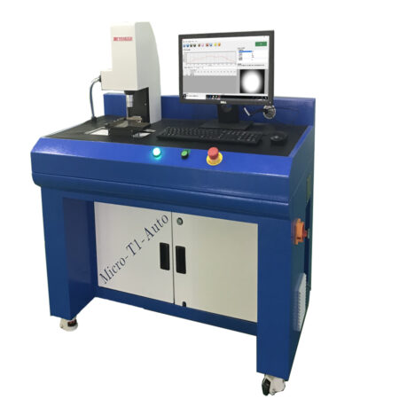
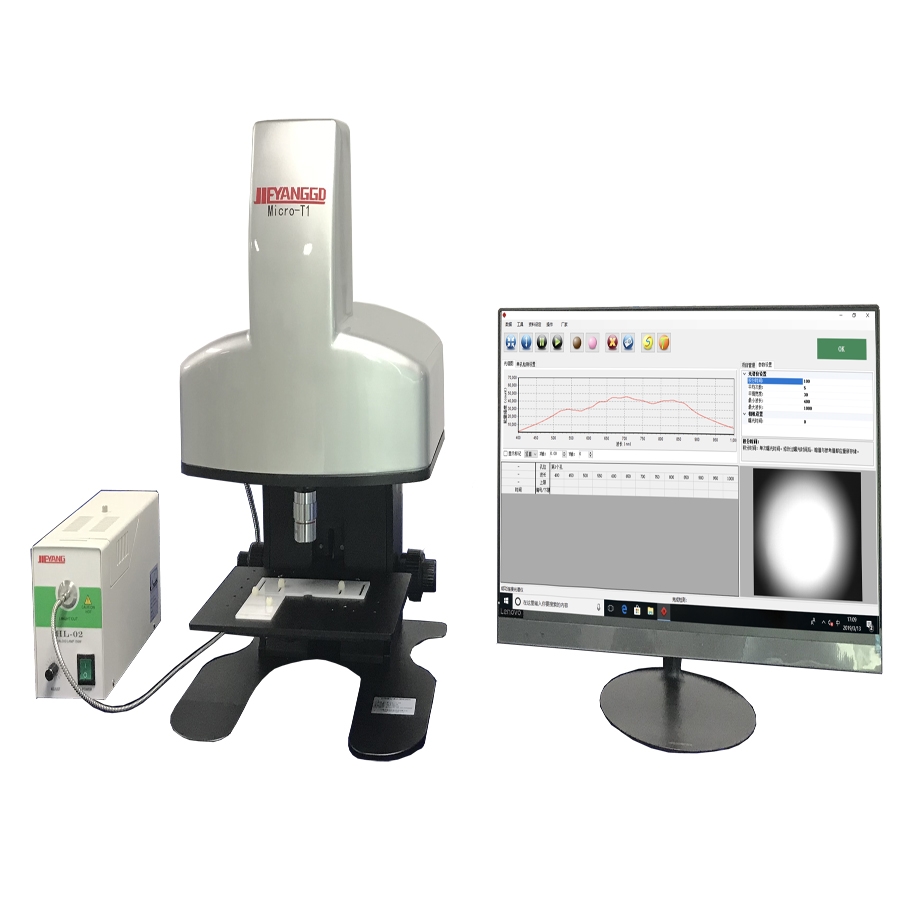
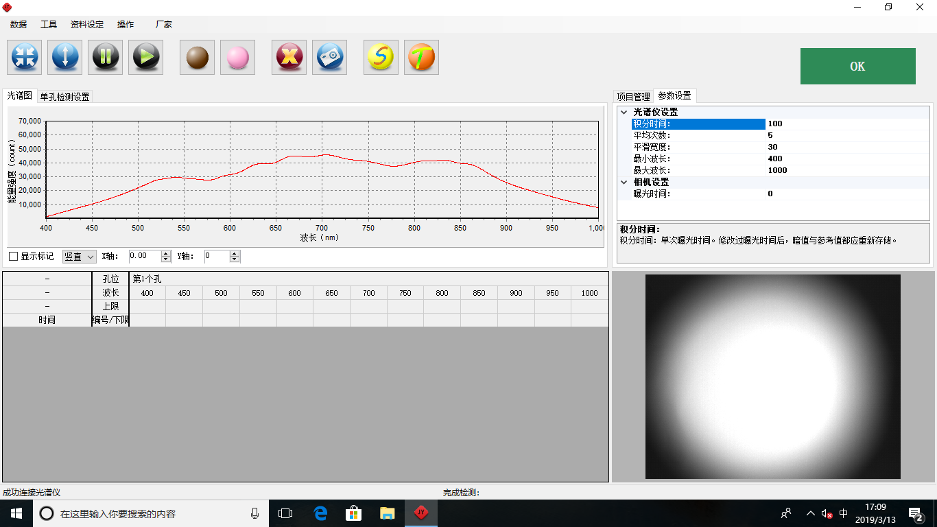
The MICRO-T1 is a visible to near-infrared micro-transmittance spectrum tester suitable for measuring the micro-transmittance of small-area planar filters, such as the transmittance detection of IR holes on mobile phone panels and the transmittance detection of remote controls. It employs a specially designed optical path that significantly enhances optical coupling efficiency, increasing the energy output by 10 times compared to standard micro-optical paths. This excellent performance meets the conditions for integrating sphere detection. Therefore, the instrument uses integrating sphere detection, eliminating the defocus chromatic aberration issues associated with ordinary lens collection, resulting in more accurate detection signals.
Ingenious Design
It utilizes a professionally designed micro-spectrum optical path, controlling the spot size within 0.15-0.5mm. The use of an integrating sphere for collection ensures more accurate and stable optical signals. Powerful operating software makes operation more convenient, and features like data recording and reporting allow users to work with greater ease.
Outstanding Performance
- Broadband Achromatic Technology
Through optimized design with multiple special lenses, chromatic aberration is controlled within a very small range across the 400-1000nm band.
- Micro Confocal Technology
The spectrum, image, and detection light sources are confocal on the object under test. While clearly.
observing the object’s morphology, the measurement light is focused on the object’s surface, and the spectral collection is focused on the same point. The collection optical path can only receive the spectrum transmitted through the sample. Light outside the focal range cannot enter the collection optical path, making the test results more accurate.
- Large Numerical Aperture Technology
Utilizing a super-large numerical aperture of 0.22, and designed for fiber optic coupling input and collection, it greatly enhances the instrument’s sensitivity.
- Integrating Sphere Collection Technology
The use of integrating sphere detection completely solves the defocus chromatic aberration problem caused by ordinary lens collection (where short and long wavelengths do not share the same focal point, preventing an optimal detection position for all wavelengths simultaneously). Our high-energy technology fully resolves this issue, with a detection time of only 100-200ms.
5.Bottom Reverse Illumination Technology
A switching structure between bottom illumination and integrating sphere collection is adopted, allowing users to conveniently observe whether the light spot accurately hits the target position, offering excellent observation results.
- Special Structural Design Technology
No need to worry about external light interference; under confocal conditions, external light cannot enter the system’s optical path.
Parameters and Configuration
|
Parameter Item |
Description |
| Sample Type |
Can measure transmittance of flat, curved, and beveled edge samples |
|
Detection Wavelength Range |
400-1000 nm |
| Wavelength Accuracy |
Less than 1 nm |
|
Wavelength Repeatability |
Less than 0.1nm |
| Detection Spot Diameter |
0.15-0.5mm (varies based on user-configured fiber and objective size) |
|
Detection Error |
Less than 0.3% (using standard reference piece) |
| Display Transmittance Resolution |
0.01% |
|
Spectrum Collection Method |
Integrating sphere collection |
| Spectrum Detector |
Back-thinned CCD spectrometer |
|
Spectrometer Optical Path Structure |
Czerny-Turner structure |
| Fastest Full Wavelength Scan Speed |
8 ms |
|
Test Hole Alignment Method |
Camera vision-assisted alignment (Observe the spot position on the IR hole via computer software to avoid manual visual error) |
| Detector Communication Method |
USB communication |
|
Light Source |
High-power halogen tungsten lamp |
| Light Source Lifetime |
2000 hours |
|
Equipment Dimensions |
400x430x630 mm |